
2026 Global Semi CapEx Map: The Divergence Between Advanced and Mature Nodes
The semiconductor industry entered 2026 with a clearer, more bifurcated capital expenditure landscape than at any point in the past decade. As hyperscalers and AI-driven computing demands continue to escalate, foundries and integrated device manufacturers (IDMs) prioritize advanced-node capacity (3 nm, 2 nm and next-generation gate-all-around architectures).
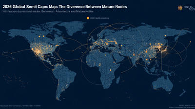
Why CapEx divergence matters
Capital expenditure decisions determine long-term capacity, competitive advantage, and regional industrial strength. Advanced nodes enable the highest performance-per-watt and the most lucrative customer relationships with hyperscalers, IDMs, and companies designing AI accelerators. Mature nodes support enormous volumes across automotive, industrial, power management, sensors, and many consumer components that require high reliability, specialized analog performance, and qualification rigor.
The divergence matters because it creates two interlinked but distinct markets: a high-margin, technology-led advanced-node market concentrated among a few players and regions, and a broad, high-volume mature-node market that underpins global manufacturing but offers lower margins and greater regional diversity. How CapEx is allocated across these markets influences pricing, lead times, local supply ecosystems (OSATs, substrates, chemicals), and national security considerations.
2026 CapEx snapshot: who’s spending and where
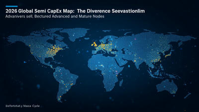
In 2026, CapEx flows show three dominant patterns:
1. Concentrated advanced-node investment: Leading-edge fabs and foundries in Taiwan, South Korea, the United States, and parts of Japan and Europe are the primary recipients of advanced-node CapEx. Investments focus on EUV tools, extreme process control, and materials for sub-3 nm nodes. These expansions are typically large, technology-intense, and tied to a small set of high-value customers—hyperscalers, cloud providers, and lead semiconductor designers.
2. Regionalized mature-node and specialty fabs: Mature node capacity and specialty fabs are expanding in geographically diverse locations including Southeast Asia, the United States, Europe, and parts of China. These investments are often smaller in scale, aimed at improving local supply resilience for automotive, industrial, and power electronics markets. They may be supported by government incentives aimed at securing critical supply chains.
3. Packaging, OSAT, and substrate investment surge: Advanced packaging (2.5D/3D stacking, chiplets, fan-out packaging) and substrate capacity see significant CapEx increases. Because advanced-system performance depends as much on heterogeneous integration as on transistor scaling, OSATs and substrate suppliers receive more strategic funding—both from private industry and public incentives—across multiple regions.
Drivers of the split: demand, economics, and policy
The CapEx divergence is driven by three intertwined forces: end-market demand characteristics, cost economics of node scaling, and strategic industrial policy. Understanding each clarifies why investment patterns differ so markedly.
Demand characteristics. Hyperscalers and AI platform builders demand the highest compute density and power efficiency, which only the most advanced nodes can deliver. These customers are willing to pay premium prices and to enter long-term partnerships with foundries. In contrast, automotive and industrial markets prioritize reliability, longevity, and qualification over cutting-edge performance; they often prefer mature nodes that match their lifecycle and ruggedness requirements.
Cost economics and margin dynamics. Advanced nodes require massive up-front investments in lithography (EUV), metrology, and R&D, but they also command higher ASPs and margins for differentiated designs. Mature nodes are cheaper to build per wafer and to operate, but they compete more on volume and efficiency, yielding lower margins. As a result, capital is concentrated where returns and strategic customer relationships promise the greatest payoff.
Policy and geopolitical motivations. Governments view semiconductor CapEx as a strategic priority. The U.S., EU, Japan, South Korea, and certain ASEAN countries have implemented subsidies, tax incentives, and direct grants to attract fabs and packaging capacity. These policies are often node- and region-specific: advanced-node incentives aim to attract high-tech fabs, while mature-node support focuses on supply resilience for critical sectors like automotive and defense.
Regional map: advanced versus mature node clusters
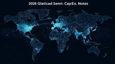
2026’s CapEx map can be read as a set of concentric clusters with overlapping influence:
East Asia (Taiwan, South Korea, Japan): Still the dominant center for advanced-node capacity and equipment supply. Taiwan and South Korea lead in high-volume advanced-node wafer fabrication and packaging integration, while Japan plays a pivotal role in specialty materials, certain equipment, and substrate supply.
United States: Growing advanced-node footprint driven by incentives and strategic partnerships with foundries and IDMs. The U.S. also focuses on specialty mature-node fabs for defense, automotive, and industrial supply chains, plus a strong push in advanced packaging and R&D ecosystems.
Europe: Selective advanced-node projects for strategic processors and automotive-grade fabs, combined with substantial investments in packaging, substrates, and equipment suppliers. EU policy emphasizes securing supply for automotive and industrial semiconductor needs.
Southeast Asia: A hub for mature-node manufacturing and assembly/test services, with incremental upgrades to support automotive and consumer electronics. The region benefits from labor-cost advantages and deep OSAT networks.
Mainland China: Significant investment across both mature and advanced segments, driven by domestic demand and strategic autonomy goals. However, access to certain advanced equipment and extreme-node supply chains remains constrained by export controls, shaping the mix of projects underway.
Packaging and OSATs: the missing link that shapes CapEx returns
Advanced packaging is increasingly the differentiator that decides whether wafer-level CapEx translates into system-level advantage. In 2026, companies investing in advanced nodes must also secure packaging capacity, substrates, and test ecosystems to realize the full value of wafer scaling. This creates a multiplier effect: regions that invest in both wafers and downstream packaging capture more economic value and talent.
Consequently, CapEx in OSATs, substrate makers, and test facilities has accelerated. Governments recognize this and often include packaging incentives in broader semiconductor subsidy programs. The net effect is a more integrated regional capability—where wafer fabs, OSATs, and materials suppliers co-locate or form trusted partnerships to shorten supply chains and improve time-to-market.
Implications for supply chain and ecosystem participants
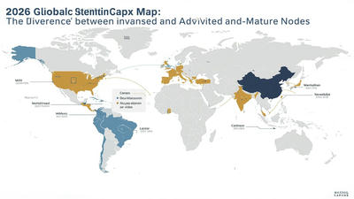
The CapEx divergence has practical implications across suppliers, OEMs, and service providers.
For foundries and IDMs: Advanced-node investments lock in strategic customer relationships but raise the bar on technical partnerships and capital intensity. Mature-node fabs must focus on yield optimization, customization for automotive/industrial needs, and cost discipline to remain competitive.
For equipment and materials suppliers: Demand is bifurcated. Makers of EUV, high-end metrology, and new materials see concentrated orders from advanced-node projects, while suppliers of mature-node process tools, chemical precursors, substrates, and test equipment service a broad set of fabs and OSATs. This split drives parallel product roadmaps and customer strategies.
For OSATs and substrate makers: These firms are in a strategic sweet spot. Investment here increases throughput for advanced systems and is often less politically sensitive than cutting-edge wafer fabs, making it a target for both private and public funding.
For OEMs and system integrators: The divergence means sourcing strategies must be nuanced. High-performance AI products will require close partnerships with advanced-node foundries and organizations that can guarantee packaging timelines. Automotive and industrial OEMs must secure mature-node capacity and long-term allocations to ensure multi-year product programs remain on schedule.
Investment themes and corporate strategy in 2026
Several investment and strategic themes dominate boardroom discussions:
Platform partnerships: Hyperscalers and large cloud providers increasingly enter long-term supply and design partnerships with foundries, de-risking revenue streams and aligning roadmaps for advanced nodes.
Vertical integration vs. specialization: Some companies pursue vertical integration—combining wafer fabs, packaging, and system design—to control timelines and margins. Others specialize and form tight ecosystems where each partner focuses on its core competency.
Geographic hedging: Firms diversify manufacturing footprints to manage trade risk and geopolitical exposure. This often means splitting mature-node volume to local fabs while concentrating advanced-node production where the most capable technology and talent exist.
Supply-chain capture: Investors target OSATs, substrate manufacturers, and specialty materials suppliers as attractive plays, since these companies benefit whenever wafer capacity scales and because they are critical to realizing wafer-level performance in systems.
Policy levers and strategic recommendations for governments
National policymakers can shape the outcome of CapEx decisions through targeted incentives and ecosystem support. Key policy levers include:
Targeted subsidies and tax incentives: Financial incentives can tip the balance for capital-intensive advanced-node projects. But policymakers should design programs that also support downstream packaging, substrates, and workforce development to maximize economic value.
Workforce development programs: Training engineers and technicians for fabs and OSATs shortens ramp times and improves yield. Public-private partnerships for vocational training and university-industry programs deliver durable talent pipelines.
Encouraging clustering and industrial parks: Co-location of fabs, OSATs, and materials suppliers reduces logistics friction and supports faster integration. Infrastructure support—power, water, transport—and streamlined permitting accelerate project delivery.
Export controls and trade policy calibration: While strategic controls can protect national objectives, overly broad restrictions can impede supply-chain collaboration and slow technology diffusion. Well-calibrated policies should balance security with commercial viability.
Risks and uncertainties on the CapEx map
Several risks could reshape the CapEx landscape beyond current expectations:
Technological disruption: Sudden breakthroughs in packaging, photonics, or materials could alter the relative value of wafer scaling versus system integration.
Macroeconomic pressure: A sharp slowdown or higher financing costs would reduce private investment appetite for capital-intensive advanced-node projects.
Policy backlashes: Geopolitical escalation may induce rapid shifts in where fabs and packaging capacity are built, which could fragment supply chains and increase duplication costs.
Execution risk: Fabrication and packaging projects often face delays, yield challenges, and cost overruns—these can change the timing and benefit realization of CapEx commitments.
Practical takeaways for industry participants
To navigate the 2026 CapEx divergence, stakeholders should consider the following tactical responses:
Foundries and IDMs: Prioritize customer lock-in through long-term contracts, co-investments, and roadmaps that align process and packaging timelines. Invest in yield and reliability programs at both advanced and mature nodes.
OSATs and substrate firms: Expand capacity strategically near leading demand centers, invest in automation to improve throughput, and diversify technology offerings to capture both advanced and mature node opportunities.
Equipment and materials suppliers: Maintain dual product streams for advanced metrology/EUV and mature-node toolsets; strengthen supply continuity for critical consumables that serve OSATs and substrate makers.
OEMs and system integrators: Develop differentiated sourcing strategies: tightly integrate with advanced-node partners for AI/high-performance products while securing long-term mature-node allocations for automotive and industrial lines.
Investors: Tilt portfolios toward firms that capture downstream value (OSATs, substrates, specialty materials) while selectively participating in advanced-node winners with defensible roadmaps and customer commitments.
Conclusion: a bifurcated future, but opportunity across the map
The 2026 global semi CapEx map shows a world of divergence: concentrated, capital-intensive investments at the cutting edge and steady, geographically distributed growth in mature and specialty nodes. This bifurcation creates distinct opportunities and challenges. Regions and firms that integrate wafer-level advances with packaging, substrates, and testing will capture a disproportionate share of system-level value. Governments that align incentives to strengthen both wafer and downstream ecosystems will accelerate local competitiveness. For industry participants, success in 2026 and beyond depends on strategic clarity—knowing when to compete in the high-stakes advanced-node arena and when to build resilient, high-quality mature-node capacity that underpins the global economy.
You May Like

Narrowing Spread Between NAND Spot and Contract Prices in 2026 – A Signal
By 2026, one of the most watched metrics in the NAND flash market has started to shift in a subtle but meaningful way: the spread between spot prices and long‑term contract prices is narrowing. For casual observers, this may look like just another incremental change in a notoriously volatile industry. For memory makers, module houses, device OEMs, and data center buyers, however, a tightening gap between spot and contract prices is a signal—a reflection of evolving supply–demand balance, risk perceptions, and strategic behavior on both sides of the market.

Price Divergence Trading Strategies Between NAND Flash and DRAM ETFs
NAND flash and DRAM sit at the core of AI storage and computing power. Both are memory, but they are not the same business. DRAM is main memory—fast, volatile, and central to high‑bandwidth workloads like AI training and inference. NAND is non‑volatile storage—slower than DRAM, but crucial to persistent data and large‑scale object storage. The cycles that drive their pricing and margins overlap, yet they often diverge. That divergence is where trading strategies between NAND and DRAM ETFs become interesting.

China’s HBM Localization Progress: The Catch-Up Pace of CXMT and XMC
China’s drive to localize advanced memory technologies has accelerated over the past several years. High-Bandwidth Memory (HBM) sits near the center of that strategy because it is integral to AI accelerators, high-performance computing (HPC) and other strategic compute platforms. Two domestic players—ChangXin Memory Technologies (CXMT) and XMC (Xianghui Memory, commonly referred to as XMC)—have become focal points in assessing how quickly China can close the gap with international incumbents on HBM die, stacking, and packaging.

Thermal Simulation Challenges and Solutions in 3DIC AI Chip Design
As AI workloads push chips to deliver ever higher compute density, designers are increasingly turning to three‑dimensional integration (3DIC) to stack dies vertically and pack more functionality into limited footprints. While 3DIC architectures unlock significant performance and bandwidth advantages, they also introduce complex thermal behaviors that are far harder to predict and manage than in traditional 2D layouts.

An Attempt at Compiling a Memory+Compute Fusion Thematic Index – A Dual-Track Framework
Most AI investors talk about “compute” as if it were the whole story: GPUs, accelerators, chips, cores. But every one of those cores needs somewhere to read from and write to. Memory and storage define how wide the data highway really is. In practice, AI performance is a fusion of compute and memory, not a solo act. So why do so many indices and ETFs separate them into different silos—one for semiconductors, one for memory, one for data centers—when the actual workloads keep blending them?

Surging Demand for Laser Drilling and Plasma Dicing Equipment in Advanced Packaging
Advanced packaging has become one of the semiconductor industry’s most important growth engines, and it is now pulling a surprising set of process tools into the spotlight. Among the most in-demand are laser drilling and plasma dicing equipment. These machines sit close to the heart of heterogeneous integration, fan-out packaging, wafer thinning, TSV formation, glass substrate processing, and other advanced flows where precision, yield, and throughput matter enormously. As packaging moves from a back-end afterthought to a strategic platform, the equipment used to shape, open, and separate materials has become just as important as the dies themselves.

D2D Interface Bandwidth and Latency Comparison in Chiplet Architectures
Chiplet architecture has turned the package into a real performance battleground. Once multiple dies are placed side by side or stacked within the same advanced package, the quality of the die-to-die, or D2D, interface becomes one of the most important determinants of system behavior. Bandwidth is no longer a nice-to-have metric, and latency is no longer a small implementation detail. Together, they shape whether a chiplet system feels nearly monolithic or frustratingly fragmented.

Stock Selection Logic and Alpha Validation of ESG-Themed Semi ETFs
Semiconductor themed ETFs are no longer just about growth and cycles. A growing subset now layers environmental, social, and governance (ESG) criteria on top of traditional sector exposure. These ESG semi ETFs promise two things at once: access to one of the market’s most powerful secular themes, and alignment with sustainability and governance standards. The pitch is appealing, but it raises two hard questions. First, how exactly are these stocks being selected? Second, does the ESG overlay help, hurt, or leave alpha unchanged?